Hardwaring around
Last year I started building my first PCB. When this article is written, the board is in production for more than half a year. No hiccups! So I count this project as a success! Design hardware in production! This is a short story about going from 0 to production in a completely new area.
The goal was to get rid of all the messy wires and have a nice PCB!
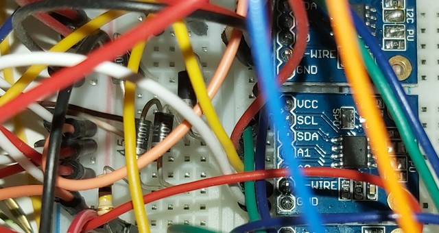
Breadboard prototyping placed in production. Worked for several years.

New PCB with nice colored resistors, mounting holes and no wires!
The board design is available on GitHub.
The faiures
Let’s start with the failures, because this is where learning happens.
“Printing” errors
While exporting the Gerber files I forgot to tick a box so some symbols are missing on the silk screen. Despite missing the component names, assembling the board was not that hard. But I had to do it with KiCad open. BOM only was not enough.

KiCad Silkscreen
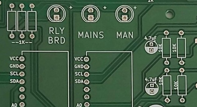
Printed silkscreen on the board. Spot the differences!
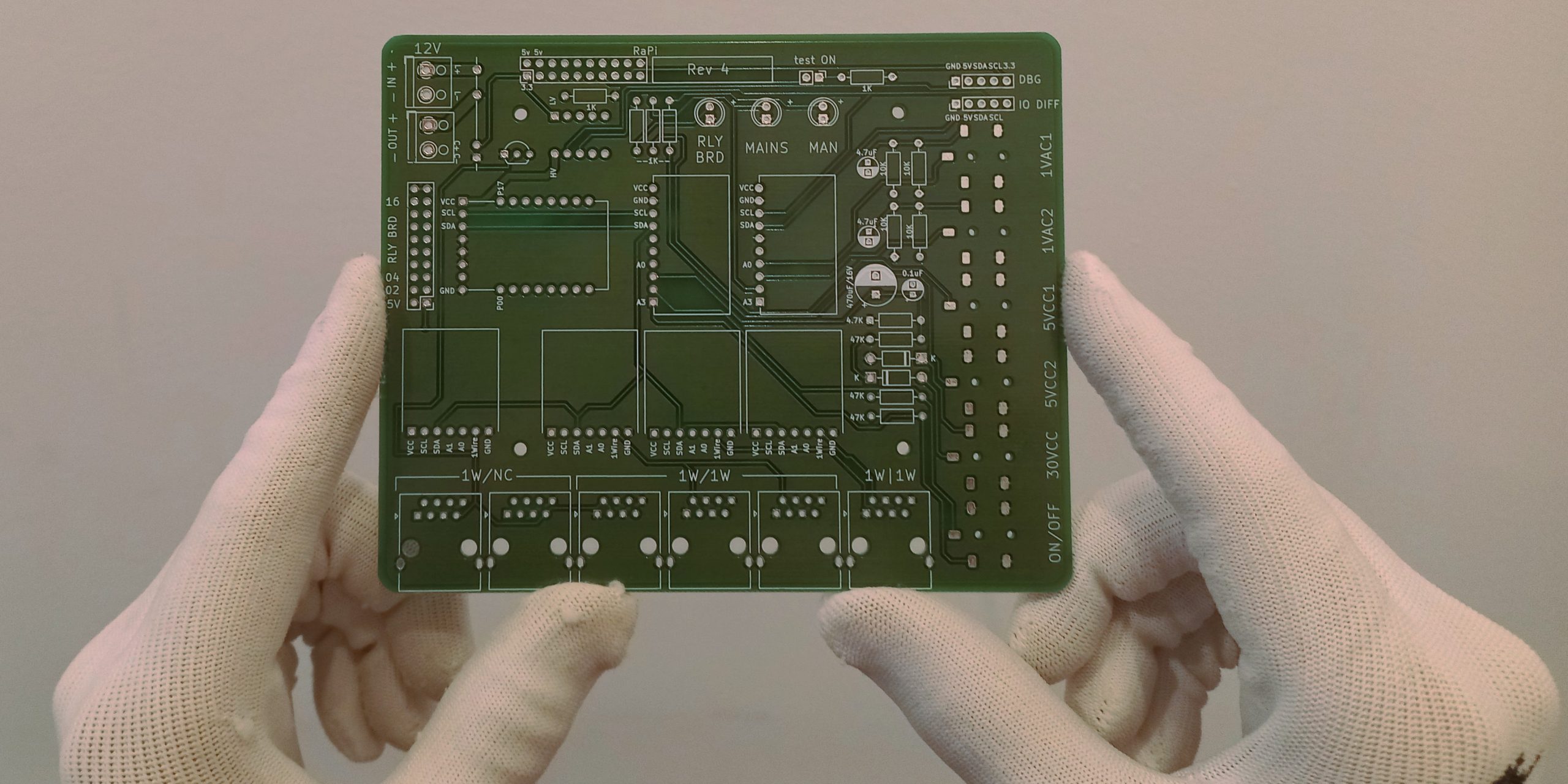
Two Layer PCB.
3D is good, if one has all the models
TME did not have THT 3.5 inch jacks so I ordered some SMD ones. Unfortunately I did not consider how thick the jack is, compared to the receiver. So I had to refactor the board!
KiCad has this nice feature where it renders the board in 3D. But only the components with an actual 3D model attached, are rendered. Except for a few passives, all the components had a custom footprint. Of course I focused all the effort on footprints, without considering building some 3D models. Maybe I would have seen the situation below, in 3D than in IRL.

3D render from KiCad

Actual board with soldered components. Note the mechanical interference.
No worries, nothing that can’t be refactored with brute force and a proper saw. Luckily I had no traces under those labels.
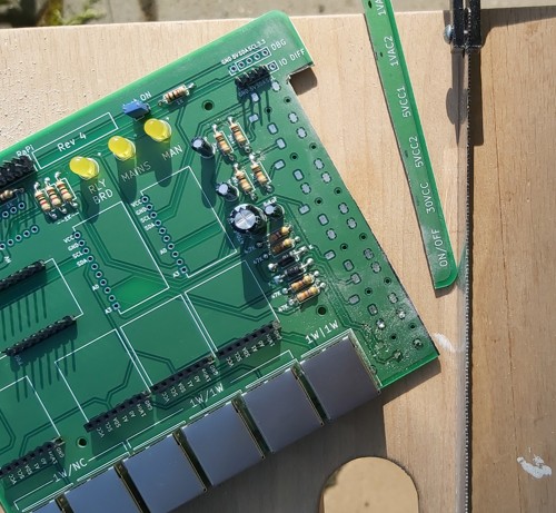
Hardware work with hardware tools
Component issues
Component shortage hits hard!
My temperature sensors are linked to Etherenet cables through RJ 45 connectors. I needed some RJ45 sockets with galvanic connection. I bought some vertical ones, not the cheapest (>1 euro/ piece), from TME. But I had the nasty surprise that they had zero [ZERO] retention! The RJ connector falls off the socket under its own weight. Luckily I had some from older projects. (The metallic sockets, in above picture)
Wrong specs are wrong
I wanted to have a UPS capability to the Raspberry. I located a 5V UPS brick from TME. On the specs, it can supply 2 Amps, at 5V, through the USB port! “Shut up and take my money!“
Well, when it arrived, I realized it couldn’t power the Raspberry properly.
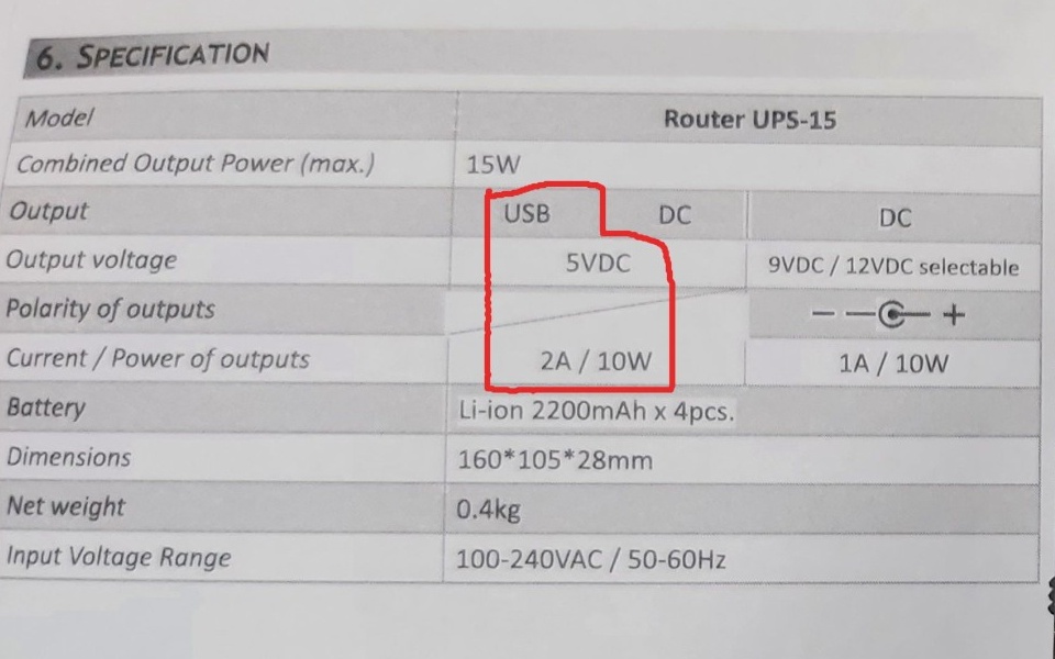
A closer look in the manual: 2A, 10W at 5V on USB output.

The label on the device: Max 1A at 5V.
So, on the manual (and on TME website) 2 Amps, at 5V on USB port. On the device, and in reality, barely 1 Amp.
The Raspberry started, glitched around, power led blinking, system logs full of under-voltage warnings. Not nice.
I wrote an email, asking if I have defective product, no answer so far. In their defense, they updated the specs on TME. And there is a more powerful model, UPS-30 than (again, according to current specs) can supply those 2 Amperes!
How did I fixed it? With a DC-DC converter and of course, bodge wires! I was “wise” enough to put a debug port (where all voltage rails were exposed) and to create a thick copper trace for 5VCC rail! Unfortunately I discovered the power brick shortcoming, way after the PCB was manufactured. Otherwise I would have integrated the DC-DC converter into the board.
The good parts
Romanian PCB service
PCB Electra manufactured my PCB. More expensive than the quote I would probably get on Chinese manufacturers but no customs! Sometimes it can take months to clear customs. One of these days, I am going to try Chinese. But not for this board.
There were no issues with tolerances, with copper traces, with silk screen. I measured the 1.1 mm 5V rail and I got 0.3 Ohm from the DC-DC output to the Raspberry Pi pin header! Here, is included the ribbon wire, the PCB trace and ~30 cm of 18AUG wire.
Footprints
Almost no part had predefined footprints. I had to make them in KiCad. I spent maybe more time drawing component footprints than “wiring” the PCB. The time spent triple checking the clearances and the part footprints, paid off greatly! Because at the mounting, they fit snugly! Awesome! And very satisfying when soldering a 12 pin RJ45! (eight plus four guidance and ground)
Community
Community is really nice! I got solid advice when asked, I even got actual hardware when complaining! Thank you VoltLog! So mind == blown! This fact alone, made the PCB manufacturing process a real pleasure!
I created a thread on EEVBlog and people answered fast and with actionable advices!
Conclusion
Were there any frictions? “Traps for young players?” [as Dave from EEVBlog would say] Except the well known component shortage, no friction. Everything worked as expected, of course, with the PCB. Hard work resulted in excellent results. There are no “silver bullets” but no dark corners/traps, at least for this low frequency, digital, THT board.
Community takes the cake! It was a pleasure asking things around, googling stuff, getting concrete advice! How much pull-up is too much for I2C? Well, here is the formula! Do I have to match trace lengths? Nope! At this frequency, no worries! Or, maybe the most money saver: You could power the Raspberry directly through pin headers!
I wouldn’t do this for a day job, but as a hobby project was awesome! Now my “Engineering stack” is a bit deeper!

